
- Industry Solutions
- Technology & Products
- Service & Support
- News
- About Us
- Qualification & Honor
- Contact Us

Digital laser direct imaging · Film-free exposure for solder mask, patterning and more
IC Substrate / FPC / HDI / Multilayer PCB · Fine resolution · Higher efficiency · Lower operating cost
Our comprehensive product line covers all major direct-write lithography applications, featuring advanced technology and precision engineering.
High-precision patterning for HDI, IC substrates, and advanced packaging.
View details →Continuous production for flexible printed circuits, up to 200 m/h.
View details →Multi-wavelength (365–425 nm) solder mask direct imaging.
View details →Full support for Fan-Out, 2.5D/3D packaging and metal fine etching.
View details →Film-free exposure — eliminates plot, develop, stabilize and retouch steps
Data files are read directly by DPX, converted into images, and the laser beam is transferred to the board through the DMD and lens.
Series peak figures — actual values depend on model configuration
Widely applied in key sectors of advanced manufacturing
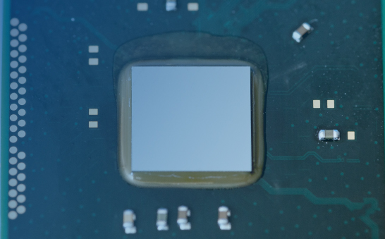 IC SubstrateAdvanced packaging substrates
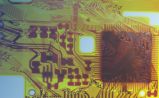 FPCFlexible printed circuits
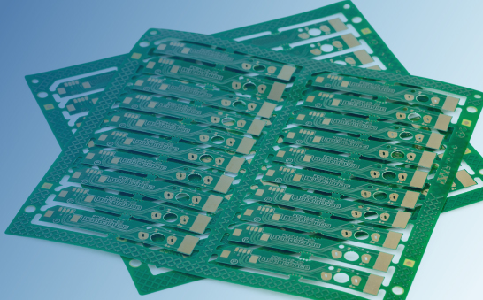 HDIHigh Density Interconnect
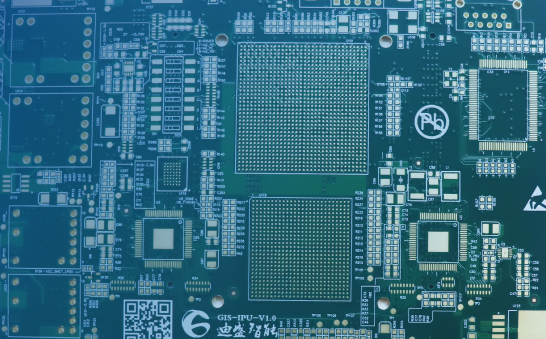 Multilayer PCBMultilayer rigid boards
Data resolution down to 0.35 µm
Min line/space 6 µm
R2R up to 200 m/h
Solder mask 5.5 panels/min · HDI 6 sides/min
10 models · 3 specification sheets · click a series card for full parameters
GIS Graphic Technology Co., Ltd.
+86 199 5132 0170 · +86 (0)512-66579218 · mk@gis-group.com.cn


