
- Industry Solutions
- Technology & Products
- Service & Support
- News
- About Us
- Qualification & Honor
- Contact Us
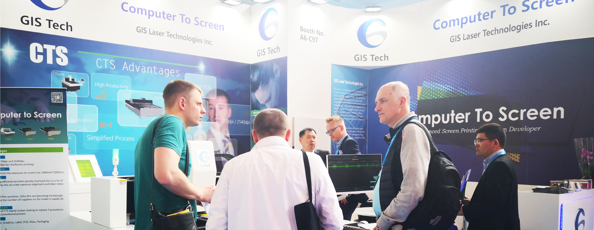
GIS Laser's Computer to Screen (CTS) Technology: Revolutionizing CTS for PCB Screen Manufacturing
In the highly precise and demanding realm of CTS for PCB screen manufacturing, every minute technological advancement holds immense significance. GIS Laser's Computer to Screen (CTS) technology, with its outstanding performance and innovative features, is gradually emerging as the technological pacesetter and leader in this field.
I. CTS Technology: A Leap Forward in Precision and Efficiency
GIS Laser's CTS technology, boasting an ultra-high resolution of 12700 DPI, shatters the limitations of traditional screen-making methods. Whether it's replicating micrometer-level fine lines or intricate details within complex graphics, CTS ensures precise reproduction with smooth, jag-free edges, laying a solid foundation for the exceptional quality of PCB products. Furthermore, this technology significantly enhances production efficiency, shortening lead times and reducing costs, thereby delivering substantial economic benefits to PCB manufacturers.
II. Intelligent Adaptation to Meet Diverse CTS for PCB Screen Needs
Acknowledging the diversity of materials and complexity of processes in CTS for PCB screen manufacturing, GIS Laser's CTS technology incorporates an intelligent expansion and contraction system. This system automatically adjusts to accommodate different material properties and process requirements, ensuring dimensional accuracy and stability for every screen. Additionally, users can flexibly set expansion and contraction parameters based on actual needs, enabling personalized production and catering to the market's demand for diverse and customized PCB products.
III. Dot Printing Technology: Elevating PCB Color Representation
In terms of dot printing, GIS Laser's CTS technology excels as well. It supports the creation of 120-line four-color screens, achieving seamless color transitions in high-density gradient areas. This technical prowess enriches PCB products with more vibrant and lifelike color representations, enhancing the visual appeal of electronic devices.
IV. High-Precision Rails and Algorithms: Ensuring Stability in CTS for PCB Screen
GIS Laser's CTS technology employs high-precision rail systems and proprietary algorithms developed by GIS Laser, achieving unparalleled control over dimensional variability during screen-making. With a remarkable dimensional variability of less than 0.005%, it guarantees precise dimensions and stability for every PCB screen, providing a reliable foundation for large-scale precision production. This high level of stability and consistency has made GIS Laser's CTS technology highly sought-after in the PCB industry.
Conclusion
GIS Laser's Computer to Screen (CTS) technology, with its precision, flexibility, and stability, is reshaping the technological landscape of CTS for PCB screen manufacturing. As a technological innovator and leader, CTS not only elevates the precision and efficiency of PCB screen-making but also opens up broader horizons for industry development. Looking ahead, GIS Laser will continue to deepen its expertise in CTS technology, bringing more surprises and breakthroughs to the PCB industry.


·CTS ·CTP ·PCB
· Flexible Surface Display Solutions
· Lithium battery automation solution
· Micro-electromechanical Systems, MEMS
· Semiconductor Packaging
 +86 19951320170 / +81-(0)80-69950298
 +86 (0) 512-66579218 / +81-(0)3-6865-8776
 mk@gis-group.com.cn / jitsuka@gis-group.com.cn