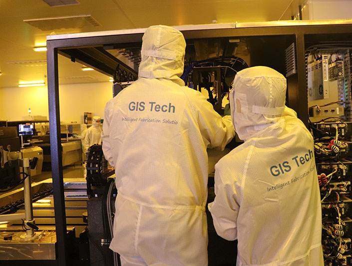
An Introduction to LDI Technology by GIS Tech
In the rapidly evolving world of electronics manufacturing, precision, efficiency, and yield are paramount. GIS Tech is at the forefront of this revolution with our advanced Laser Direct Imaging (LDI) systems. Here’s how this groundbreaking technology works and why it provides a superior alternative to traditional photolithography.

How Does LDI Work? The Principle of Digital Direct-Write
Traditional PCB exposure relies on physical phototools (film masks). These films are placed over a light-sensitive substrate and exposed with UV light. This process is prone to errors from film handling, misalignment, and environmental changes.
LDI technology eliminates the phototool entirely, acting like a high-precision digital printer for circuit patterns.
The LDI Process Breakdown:
Data Input: The digital circuit design (e.g., Gerber file) is directly uploaded to the LDI system.
Laser Generation: A high-power, stable ultraviolet (UV) laser source inside the system generates a laser beam.
Spatial Light Modulation (The Core): This is the most critical step. The laser beam passes through a Spatial Light Modulator (SLM), typically a Digital Micromirror Device (DMD). The DMD contains millions of microscopic mirrors. Each mirror corresponds to a pixel and tilts to either direct light onto the substrate ("on") or away from it ("off"), effectively "drawing" the circuit pattern with light.
Precision Scanning & Exposure: The modulated laser pattern is focused through a high-resolution optical lens system and is precisely scanned across the PCB panel coated with photoresist (solder mask or line ink).
Chemical Change: The UV laser energy causes a photochemical reaction in the exposed areas. During subsequent development, the unexposed (or exposed, depending on the resist type) areas are washed away, revealing the exact circuit pattern.
In short: LDI replaces physical film with a dynamic, digital mask of light.
Key Advantages of LDI Technology
By moving to a all-digital process, LDI offers transformative advantages:
Unmatched Precision and Resolution:
Eliminates phototool-related errors like wear, stretch, and misregistration.
Enables the production of extremely fine lines and spaces (down to 15μm and below) and perfect layer-to-layer registration, which is critical for HDI, IC Substrates, and Mini LED manufacturing.
Superior Yield and Process Stability:
The non-contact process prevents scratches and defects caused by handling physical films.
Digital consistency ensures every panel is identical, dramatically increasing overall yield.
Increased Efficiency and Flexibility:
Dramatically reduces time-to-production by eliminating the time needed to produce, handle, and align phototools. This is a huge advantage for quick-turn prototypes and high-mix production.
Allows for last-minute design changes with no cost or delay for new films.
Significant Cost Reduction (Cost Down):
Eliminates direct costs associated with phototool fabrication, maintenance, and storage.
Reduces indirect costs by minimizing scrap and rework due to phototool errors.
Environmentally Friendly:
Removes the need for chemicals used in film development and cleaning.
Why Choose GIS Tech's LDI Systems?
GIS Tech has established itself as a leading domestic manufacturer of LDI equipment by integrating these core advantages into robust, high-performance machines designed for the modern PCB factory.
Proven Performance & Reliability: Our systems utilize high-quality UV laser sources and precision DMD modules to deliver exceptional imaging accuracy (<±10μm registration) and stability for 24/7 industrial operation.
High Productivity: Designed for high throughput, our LDI systems can process dozens of panels per hour, maximizing your capital investment and meeting tight production schedules.
Superior Cost-Effectiveness: GIS Tech provides performance that rivals international brands but at a more accessible price point, with significantly lower total cost of ownership.
Exceptional Local Support: Our greatest advantage is our local presence. We provide rapid, on-the-ground technical support, process optimization, and maintenance services, ensuring minimal downtime and maximum productivity for our customers.
Wide Application Range: Our LDI systems are trusted by manufacturers in various segments, including HDI, Flexible Circuits (FPC), IC Substrates, and Advanced Packaging.
In summary, GIS Tech's LDI systems represent the future of PCB imaging. By harnessing the power of digital direct-write technology, we empower manufacturers to achieve new levels of precision, efficiency, and profitability, solidifying their competitive edge in the global market.


